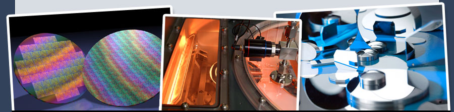
Foundry Services
Silicon Sense supplies foundry services to a wide range of companies for a multitude of private and commercial applications. We provide the best silicon wafers to support their manufacturing or development projects. Silicon Sense also offers micro machining as a service.
Foundry services include:
- Thermal Oxidation (wet and dry)
- LPCVD (low stress nitride, super low stress nitride, stoichiometric nitride)
- PECVD (oxynitride, low stress nitride, oxide, carbide)
- Metalization (DC and RF sputtering, evaporation coatings)
- Dry etch
- Grinding, lapping and polishing to exact tolerances and specifications
- Ultrasonic and micro machining
- Wafer dicing (automated sawing and cleaving)
- Microsystems engineering
We can accommodate small and large quantity requests with diverse specification requirements. If you do not see a service listed, give us a call or simply fill out the request for quote form. Our representatives are ready to assist you!